Reactive Ion Beam Etching RIBE is a technique well suited to etching slanted features. The technique allows localized removal of material using a broad ion beam. The material is removed at the wafer surface following collisions between accelerated ions and reactive species formed in the ion source. Control and repeatability in defining slanted features are contingent on advanced Ion beam source configuration and experienced selection of processing conditions.
In this paper, we describe how Oxford Instruments Plasma Technology solution delivers controlled processing of slanted gratings used as light coupler for Augmented Reality waveguide combiners. We demonstrate control of the slant angle, the groove depth, and the filling ratio for large wafer sizes.
High Uniformity of the Etching Depth at Slanted Angles
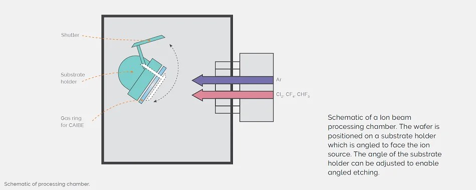
Plasma Technology solution for uniform etching is based on RIBE etching of an angled substrate. Control of the slant angle is enabled by Plasma Technology’s custom made highly directional ion beam combined with an adjustable substrate holder tilt controlled to 0. Currently, the slanting angle is controlled from 35° to 60°. When etching slanted features, the angled position of the substrate causes non-uniformity of the etch depth which becomes more difficult to control without rotating the substrate.
To achieve uniform etching over a large area, our proprietary hardware design compensates for non-uniformity in the ion flux. This design allows for the optimization of the local etch uniformity over a range of angles. To demonstrate a large processing area with excellent uniformity, a 200 mm SiO2 on Si wafer was etched. The results demonstrate an excellent uniformity for slant angles ranging from 35° to 55° deg. The graph below shows full wafer data for grating angles 35°, 45°, and 55°.
 Want to know more? Click here to read the full article.
.jpg)
This information has been sourced, reviewed and adapted from materials provided by Oxford Instruments Plasma Technology.
For more information on this source, please visit Oxford Instruments Plasma Technology.